Open Access
Research Article
Max Screen >>
ISSN: 2348-9812
Copyright: © 2017 Altinoluk SH. This is an open-access article distributed under the terms of the Creative Commons Attribution License, which permits unrestricted use, distribution, and reproduction in any medium, provided the original author and source are credited.
Related article at Pubmed, Google Scholar
Surface texturing is an indispensable process for solar cell fabrication. The interaction of the surface with the incoming sunlight is controlled by texturing in such a way that the absorption is maximized through multiple interactions. Wet and dry etching techniques have been used to create textured surfaces on solar cells. Other than standard alkaline texturing used by the industry, metal assisted etching (MAE) appears to be a promising texturing technique with greater potential application for multi-crystalline solar cell fabrication. It is possible to achieve both random and periodic patterns with MAE which is relatively cheaper than dry plasma etching techniques. In this study, periodic hole patterns with micron sized diameters and periodicity were aimed to be achieved. Etching rate was shown to be strongly dependent on the surface orientation. Uniformly distributed patterns with various diameter and period values were successfully obtained. Fabrication of solar cells on these surface patters were demonstrated. Performance of solar cells was evaluated through parameters like efficiency, open circuit voltage and short circuit current.
Keywords: Surface texturing; Light trapping; Metal assisted etching; Periodic patterning; Micro and nano hole texturing of crystalline silicon surface
Serra Altinoluk was born in 1983 in Mersin, South Turkey. She got her bachelor and master degrees both in Electrical and Electronics Engineering Department at Mersin University, at 2005 and 2007 respectively. In 2008 she joined to Middle East Technical University, started working as project assistant at Electrical and Electronics Engineering Department. In 2012 she started working as a research assistant in Center for Solar Energy Research and Application, doing her PhD with her supervisor Prof. Rasit Turan. From April 2014 to September 2014 she visited Arizona State University, and later IMEC as a visiting researcher to carry out some of her PhD work.
In order to create a sustainable future for our planet while supplying continuously increasing energy demand of our society, we should use clean energy resources rather than burning fossil fuels like coal, natural gas, and liquid oils. Among the renewable and clean energy sources, solar energy has the greatest potential for providing all energy needs of the human being today and in the future. However, it is required to develop technologies to convert solar energy to other forms like electrical and mechanical energies with high efficiency and low cost. Thus, increasing solar cells efficiency and lowering the material and process costs are the main aim in most of the research efforts. Surface texturing is an indispensable method for light harvesting to develop high efficient solar cells. Metal assisted etching method offers a new and industrially compatible alternative for creating a variety of surface structures that may lead to better performances when compared with conventional pyramid textured counterparts. This work presents some new results on surface texturing by metal assisted etching.
In general, texturing of the Si wafer surface is performed by creating random pyramids through anisotropic etching process [1]. Although random pyramid texturing is the most common approach for surface texturing today, many research groups focus on alternative structures on the surface to reduce material consumption during the texturing process together with improved light trapping performance. The problem with random pyramid texturing is, the height of the pyramids. The thickness of the substrate is comparable with the height of the pyramids, which makes it impossible to carry out further processes with the substrate. Researchers seek for alternative texturing techniques to overcome material consumption and having to work with thick substrates. Structuring the Si surface by periodic and random cones, rods, wires and holes have already been studied by several research groups [2-5]. For solar cell application, the texture is expected to improve the solar cell performance and decrease the cost of fabrication process. Aforementioned textures have both cons and pros. Rods are freestanding parts of substrate and for tall rods, there is a high possibility of their getting broken. The diameter of the wires is around nanometer level, which makes it very complicated during passivation studies. Wire texturing will end up with optically great, but electrically poor output devices. Among the surface geometries studied, periodic hole patterns were reported to be the most promising structure for an effective light trapping [6]. Unlike rods, holes can freely stand and make it possible to work with thin substrates. The scope of this study is to investigate the use of metal assisted etching (MAE) to create periodic hole patterns on Si wafer for solar cell applications. It is aimed to increase optical performance of the solar cell while keeping electrical losses as small as possible. In this paper, we report on patterning of crystalline silicon (c-Si) surface by MAE which is a wet chemical etching method for the fabrication of random and periodic structures with the help of catalytic effect of metals. Metal layers can be used as both direct catalyst and mechanical support [7].
In order to obtain periodic patterning, there should be a lithography step. With optical lithography, we can define the pattern of the textures on the surface and during etching step predefined parts of the surface will be etched. For random texturing, there is no need for the definition of patterns. MAE was used as an electroless etching technique utilizing a discontinuous layer of metal in suitable oxidant such as hydrogen peroxide (H2O2) and hydrofluoric acid (HF) to obtain porous Si and porous III–V compound semiconductor by Li et. al. in 2000 and 2002 in contrast to the conventional anodic etching method for porous semiconductor formation [8]. During MAE, noble metals are used to initiate local oxidation and reduction reactions [9]. Metals such as gold (Au), platinum (Pt) and silver (Ag), deposited on the surface of a semiconductor (e.g. Si) serve as a local cathode to catalyze the reduction of oxidants (e.g. H2O2) producing holes. Random and periodic patterns can be obtained with the help of noble metals and appropriate chemical components [10].
Schematic representation of periodic hole array formation with metal assisted etching process is shown in Figure 1. The hole pattern was first defined by the photoresist through a lithography process regardless of orientation. A thin layer of Ag was then evaporated on patterned surface which is followed by a lift off process which left behind circular metal dots on the surface shown in Figure 1-b. During MAE, Si under metal dots was etched away through chemical reactions described elsewhere, array of holes was then formed. In the final step of MAE process, the residual metal was removed using aqua regia solution [11].
In this study, p-type Si wafers with both (111) and (100) orientations and resistivity of 1-5 Ω-cm were used. Fabrication steps of a standard solar cell with aluminum back surfaces field (Al-BSF) is shown in Figure 2. The standard solar cell fabrication process starts with RCA cleaning (5 H2O+ NH4OH + H2O2) [12]. After the cleaning step, depending on the dimensions of the textures aimed to be created on top of the surface, appropriate resist is selected. Depending on the diameter and the pitch sizes of the holes, unique lithography recipes have been developed. During MAE silicon deposited with metals is immersed into HF/H2O2/H2O solution, where metal coatings facilitate the etching [13]. Thanks to the novel electrochemical properties of the interaction between Si and active noble metals, there is an electrokinetic model which satisfactorily explains the microscopic dynamic origin of motility of metal particles in Si. According to this model, the power generated in the bipolar electrochemical reaction at a metal particle’s surface can be directly converted into mechanical work to propel the tunneling motion of metal particles in Si [14,15]. The chemical and electrochemical reactions occurring preferentially near the noble metal can be briefly defined as:
• At the cathode (the metal): H2O2 is reduced as H2O2 + 2H+ → 2H2O + 2h+
• At the anode (the silicon substrate): The Si substrate is oxidized and dissolved. Although the reaction is controversial, there are three main models proposed for the dissolution process of Si as given below :
Si + 4h+ + 4HF → SiF4 + 4H+ & SiF4 + 2HF → H2SiF6
Si + 4HF-2 → SiF2-6 + 2HF + H2 ![]() + 2e-
+ 2e-
Si + 2H2O → SiO2 + 4H+ + 4e− & SiO2 + 6HF → H2SiF6 + 2H2O
The most critical feature of this reaction scheme is the generation of h+ from H2O2 and the reduction of H+ to form H2, both of which are facilitated by the metal particles [13,16]. After wet chemical etching, remaining metals have been removed with aqua regia (nitric acid + hydrochloric acid = 1:3). Following metal removal step, wafers were doped with P using POCl3 at temperatures lower than 850° C. After P diffusion, silicon nitride (SiNx, Si-rich where 0 A wide range of hole diameter and distribution was studied from micron to submicron levels [17]. Resist coating recipe was optimized according to required hole diameter and the pitch (periodicity) values. The schematic representation of a hole textured surface including dimensions is shown in Figure 3. In principle, chemical etching techniques are dependent on the surface orientation due to the fact that the bonding energy of the surface atoms can be very different for different crystallographic direction. The (111) surface has two surfaces with atoms having one free bond ending up with a low surface energy, one with very high activation energy due to three back bonds. On the contrary, (111) surface has lower activation energy [10]. For this reason, (111) oriented wafers have usually lower etch rate values compared to (100) orientation [18]. In order to see the degree of orientation dependence of MAE patterning, we performed a series of simultaneous experiments for (100) and oriented wafers. Figure 4 shows the depth of the holes created by MAE as a function of etching time for the sample having 3 μm hole diameter and 6 μm pitch size. The etch rates for this particular case were found to be 0.13 μm/min and 0.43 μm/min for (111) and (100) orientations, respectively. Large difference between etch rates of these two orientation is consistent with the expectation. Figure 5 shows representative SEM images of the holes having same diameter and variable pitch sizes. These patterns were prepared on the same wafer and subjected to same process conditions. We see that hole patterns with perfect circular shapes and different distribution are formed with MAE. In some cases additional patterns, randomly distributed wire inside holes, were observed in the hole as shown in Figure 5. The control of the diameter and the pitch size is quite well so that the intended geometries can be achieved without any deformation. It is however clear that formation of deep holes are hardly possible with (111) surface orientation due to the low etch rates. Figure 6 represents the SEM images of surfaces obtained after MAE process. The wafers shown here were having (111) orientation. The diameter of the predefined holes was 3 μm, thanks to successful lithography recipe to end up with desired distribution of holes, diameter and pitch sizes. Optical properties of the patterned surface were studied through reflection measurements as shown in Figure 7. Samples used in this study have the hole diameter of 5 μm and the pitch sizes of 6, 8, 10 μm. It can be seen that the lowest reflection value was obtained from the sample having the smallest pitch size. The reflection from this sample is even lower than the pyramid textured samples. The texture with the lowest pitch size refers to the sample with the most dense surface having the highest hole volume on top of the surface. For optical performances the surfaces textured with MAE were analyzed without SiNx coating, on the other hand electrical performances of the solar cells were obtained after standard solar cell fabrication steps including antireflection coating. I-V curves of the solar cells fabricated on the sample with 5 μm diameter are shown in Figure 8. Solar cell parameters extracted from these curves are tabulated in Table 1. It can be seen that solar cells with reasonably well I-V curves have been obtained on hole textured surface. The effect of hole distribution is mostly pronounced in the short circuit current (Jsc) value which increases with increasing pitch size significantly. Highest values were obtained with largest pitch size and the deepest structure which correspond to lowest hole density on the surface. This result indicates that the charge collection efficiency worsens with increasing hole volume on the surface. On the other hand, the open circuit voltage (Voc) value was found to be less sensitive to the pitch size. It is however lower than one might expect from a c-Si solar cell device. This is due to the poor surface quality after MAE process. In this work we have not attempted to optimize surface passivation. An effective surface passivation would improve the open circuit voltage significantly. In addition to better passivation optimizations, with the fabrication of deeper structures, with aforementioned pitch sizes, it is clear that we can end up with better cell performances [18,19]. 2 μm in diameter and 23.2 μm in length with a better passivation process step ended up with 13% of cell performance [9]. Unlike our resist coating technique, surface patterning was conducted with circular shaped photoresist dot arrays and optimized antireflective coating process step [9]. The solar cell performances shown in Table 1 were subjected to process steps shown in Figure 2. Nano wires inside the holes can be eliminated with an additional chemical process in order to obtain smoother hole textures especially for (100) oriented wafers. Although these unintended textures ended up with lower reflection values, they were difficult to be passivated. This problem can be solved with improved passivation process step. Atomic layer deposition process can an alternative passivation technique for textured surfaces. We have successfully employed metal assisted etching technique to create periodic hole patterns on Si wafer as light trapping medium in solar cell applications. As expected, etch rate along (111) direction was found to be significantly slower compared to that along (100) direction. Thus (100) orientation provides us with a wider range of surface dimensions for MAE texturing studies. Performance of solar cells with hole patterns has been evaluated through different hole pitch sizes. We have observed that the cell performance improves with increasing pitch size as a result of less hole density. The open circuit voltage is generally low due to the poor surface quality and found to be less sensitive to the hole distribution. By eliminating the wires inside the holes and with better optimization of antireflection coatings and metallization schemes, the solar cell performances are expected to improve more.Dependence of Etch Rate on Orientation During MAE
Solar Cells Textured with MAE
Discussions
Conclusion and Future Work

![]()

 |
Figure 1: MAE process sequence with periodic patterning a) Surface patterning, b) Metal evaporation, c) Wet chemical etching and removal of resist and metal residuals |
 |
Figure 2: Process flow of solar cell fabrication with periodic hole textured front surface: a) cleaning of the wafers, b) photoresist coating with appropriate recipe depending on the dimenison of the textures, c) photolithography, d) MAE process, duration is defined according to the desired texture depth, e) photoresist and metal removal, f) doping, g) antireflection (SiNx) coating for passivation, h) metallization with Ag for front and Al for back contacts, i) edge isolation |
 |
Figure 3: Schematic representation of radius (r), pitch (p) and length of the sample (L) |
 |
Figure 4: Etch rate comparison of wafers having 3 µm hole diameter and 6 µm pitch size coated with 25 nm Ag having (100) and (111) orientations |
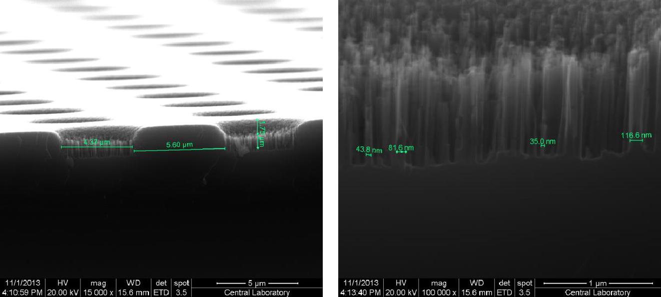 |
Figure 5: SEM image of (100) oriented wafer with 5 µm diameter and 9 µm pitch size |
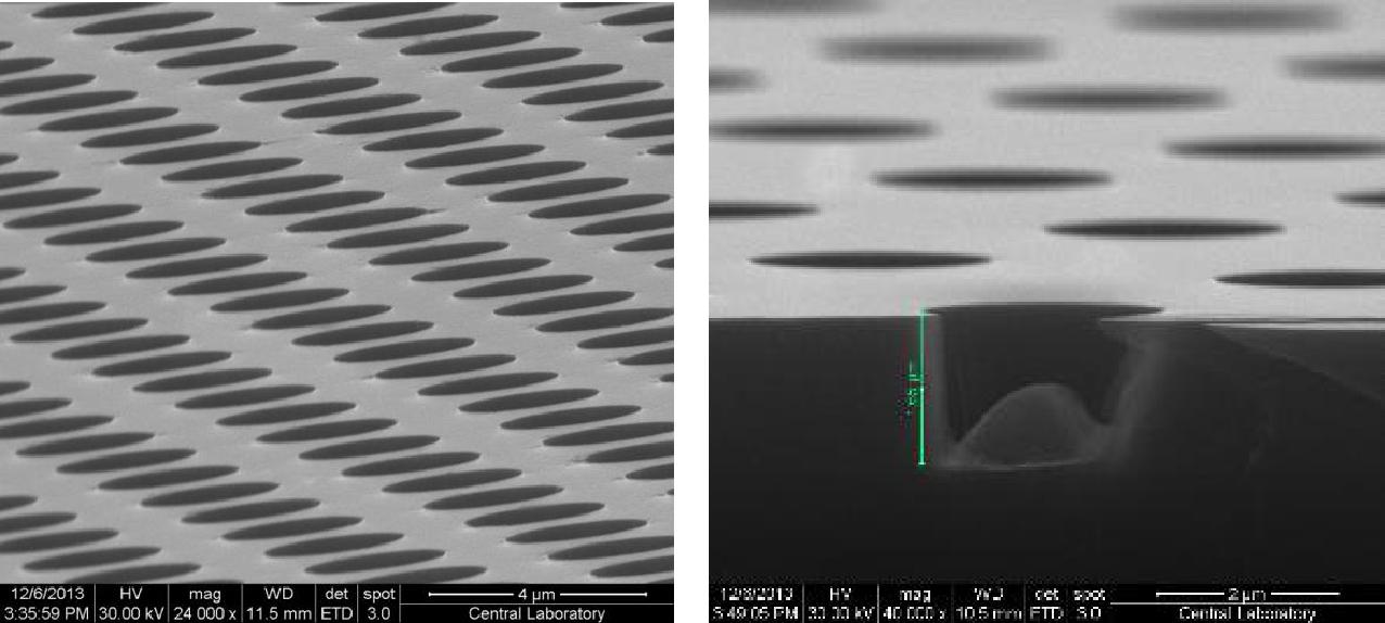 |
Figure 6: SEM images of (111) oriented wafer with 3 µm diameter and 5 µm pitch size |
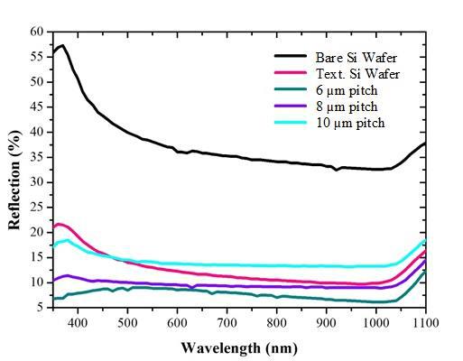 |
Figure 7: Reflection spectra comparison depending on holes with 5 µm diameter and 6, 8, 10 µm pitch sizes. Sample with pyramid textures made by alkaline etching is also shown (pink curve). No antireflection coating was applied to these samples |
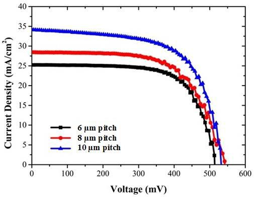 |
Figure 8: Current density versus voltage graphs of samples with 5 µm diameter and 6, 8, 10 µm pitch sizes subjected to one hour wet chemical etching |
Diameter: 5 μm |
Depth (μm) |
Voc (mV) |
Jsc (mA/cm2) |
FF (%) |
η (%) |
6 µm pitch size |
17.48 |
512.1 |
25.2 |
69 |
8.9 |
8 µm pitch size |
19.32 |
531.6 |
28.4 |
64.1 |
9.6 |
10 µm pitch size |
23.04 |
531.8 |
34.1 |
63.7 |
11.5 |
Plane |
-- |
564.9 |
20.9 |
75.8 |
9 |
Table 1: Performance parameters of solar cells textured with 5 µm diameter holes and 6, 8, 10 µm pitch sizes |
|||||