Open Access
Research Article
Max Screen >>
ISSN: 2348-9812
Copyright: © 2016 Bonomo M. This is an open-access article distributed under the terms of the Creative Commons Attribution License, which permits unrestricted use, distribution, and reproduction in any medium, provided the original author and source are credited.
Related article at Pubmed, Google Scholar
Mesoporous NiO films obtained via screen-printing deposition of a newly formulated paste containing preformed NiO-nanospheres have been employed as nanostructured photocathodes of p-type dye-sensitized solar cells (p-DSCs). The novel aspect of this contribution is the utilization of a diluted solution of weak acid as anti-aggregating agent of NiO nanoparticles during the preparation of the screen-printing precursor. Screen printed NiO cathodes of p-DSCs displayed photoactivity in both bare and sensitized states with overall efficiencies not higher than 0.05% when erythrosine b (ERY) was the colorant and I3-/I- the redox mediator. The charge recombination resistance of NiO photocathodes in the illuminated p-DSCs diminished from 230 to 90 Ω with the increase of cell efficiency in going from the pristine oxide to its ERY sensitized version. In absence of a redox mediator, the NiO electrodes here considered displayed electroactivity due to the occurrence of solid state oxidation processes in the range 0.1-1.0 V vs Ag/AgCl. From the modelling of the electrochemical impedance data the total electrical resistance Rtot of screen printed NiO decreased drastically in passing from the pristine (1*105 - 6*105 Ω) to the oxidized state (20 - 150 Ω). The fitting parameter Rtot combined the two terms of bulk transport and charge transfer at the NiO/electrolyte interface. Rtot depended on NiO film thickness and on the nature of the electrolyte in a non-straightforward manner for the verification of electrochemically induced processes of NiO film dissolution.
Keywords: Nickel Oxide; DSC; Photoelectrochemistry; p-type
In the ambit of photovoltaics as more credible and truly sustainable alternative to the utilization of the primary energy source of fossil fuels, the dye-sensitized solar cell (DSC) [1] and it’s more recent concurrent perovskite-based solar cell [2,3] are no longer interesting and promising newcomers that started as a little bit more than an “ugly duckling” in comparison to the “swan” Si-based pn junction, but well characterized and developed devices with quite high efficiencies (now comprised between 12-13 % for a DSC [4,5] and 21 % [6] for a perovskite solar cell in their most performing configurations). Such excellent performances generally suffer of a poor reproducibility and, most of all, time stability on a timescale larger than 1 or maximum 2 years of utilization in ambient conditions [7] when no treatment of artificial ageing is applied. In the context of DSCs the devices employing photoactive n-type nanostructured semiconductors [8] represent the excellence being by far the most performing ones [5] with the display of the largest values of overall conversion efficiencies. It is relatively recent the interest towards p-type DSCs utilizing photoactive nanostructured semiconductors with holes as majority carriers either in the single photoactive electrode configuration [9-12] or in the tandem configuration (t-DSC) in which photoactive anodes are coupled with photoactive cathodes [13-16]. The main motive of interest towards increasingly efficient DSCs with p-type photoelectrodes is the possibility of achieving theoretical conversion efficiencies 1-2 times larger for t-DSCs [17-19] with respect to the related photoelectrochemical cells employing separately the two photoactive electrodes [20]. In fact, the combination of a photoactive cathode with a photoactive anode in the same DSC brings about the increase of the open circuit photovoltage in comparison to the corresponding values measured with photoelectrochemical cells having single photoactive electrode [13,21].
As widely acknowledged, the evolution of the p-DSCs has been consequential to the improvement of the properties of mesoporous nickel oxide (NiO) electrodes since this material constitutes the photoactive cathodic material of p-DSC par excellence [22]. With the exception of very few cases (e.g. CuAlO2, CuGaO2, CuCrO2 or KxZnO), [23] the progress on p-DSCs is practically based on the improvement of the methodologies of NiO thin film preparation/deposition,[24] and on the synthesis of optimized dye-sensitizers specifically designed to match their HOMO-LUMO levels with the frontier energy levels of nanostructured NiO cathodes [25-27]. In the present work we focused on the electrochemical characterization of screen-printed NiO thin films with mesoporous morphology in three-electrode cells containing only the metal oxide as solid state electroactive species. These materials in the configuration of thin films were successively tested as photoactive cathodes for DSCs. The method of deposition of the NiO samples here considered is screen-printing [28] from a paste with predefined chemical composition. Screen printing is based on the uniform spreading of a viscous paste containing either the metal oxide as dispersed nanopowder, or the oxide precursors. The advantages of the screen-printing method for thin films deposition are the scalability, homogeneity and uniformity of the resulting deposits, the possibility of modulating the chemical composition of the paste and the easiness of purification [11]. Paste spreading is realized onto transparent conducting materials (TCS) like indium-doped tin oxide (ITO) [29] or fluorine-doped tin oxide (FTO) [30] substrates which allow at the same time the transmission of the optical radiation necessary to activate the photoelectrochemical processes, and the electrical connection of the cell to an external circuit. The deposited paste is heated by means of a controlled ramp of temperature to remove the volatile components whereas the sole oxide remains on the fired substrate at the end of the thermal treatment. In the case of NiO deposition, sintering temperature cannot exceed 450 oC [24]. Such an upper limit allows the achievement of a deposit of metal oxide with an elevated extent of mesoporosity while maintaining a good level of adhesion on the substrate. Moreover, the thermal treatment carried out below 450 oC warrants the electrical connectivity within the skeleton of NiO, and at the interface NiO/TCS [31]. Our research group has recently proved the feasibility of the screen-printing method for the preparation of mesoporous NiO cathodes displaying photoelectrochemical activity when NiO thin films were sensitized with erythrosine b (ERY) and with a series of newly synthesized squaraines [11]. In that work the screen-printing deposition of NiO was realized by adapting the method commonly used for the preparation of titania films for DSC purposes from commercial precursors [28]. The aspect of novelty of the present work is represented by the evaluation of the influence of the chemical composition of the paste on the electrochemical/photoelectrochemical properties of screen printed NiO when the procedure of sintering is the same. In particular, the new paste here adopted for the screen-printing deposition of NiO differs from the previous versions for the amount of the acidic component in the starting mixture of paste precursors. The analysis of the photoelectrochemical properties of this new NiO sample sensitized with ERY colorant as benchmark [13] will be presented. This type of analysis is generally rendered difficult by the simultaneous occurrence of redox processes based on NiO and on the redox shuttles in the actual solar conversion devices [23,31-33]. For this reason it is fundamental to characterize these complex electrochemical systems in absence and in presence of the redox couple for distinguishing the electrochemical processes based on sole NiO from those originated from the shuttle.
The preparation of the NiO paste for the successive screen-printing deposition process is carried out through a multistep procedure as reported in Table 1. This procedure is a slightly modified version of the one reported by Ito et al. [28] who described the preparation of TiO2 pastes to be utilized in the deposition of mesoporous photoactive anodes for DSC of n-type. All chemicals were purchased from Sigma-Aldrich or Fluka at the highest degree of purity available and were used without any further purification. Anhydrous terpineol (step 7 in Table 1) was added as a mixture of enantiomers. Grinding of the various mixtures obtained at the different steps (1-3, Table 1) was conducted at room temperature and ambient conditions with a mortar having a diameter of 15 cm. Stirring was carried out with a 4 cm long magnetic stirrer at rotation speed of 250 rpm. The preparation of the paste here reported is characterized by the utilization of a double amount of glacial acetic acid in the first step of NiO nanoparticles dissolution (Table 1) with respect to the previously reported procedures [11,28,34].
The ultrasonic homogenization (steps 8 and 10, Table 1) was performed with a Ti-horn -equipped sonicator (Vibracell 72408 from Bioblock scientific). The final paste had the appearance of viscous slurry and was stable up to one year. This modus operandi represents one of few processes that starts directly from preformed NiO nanospheres (max diameter = 50 nm, from Sigma-Aldrich) instead of NiO chemical precursors as NiCl2 or Ni(OH)2, for the preparation of the nickel oxide paste.
The paste containing preformed NiO nanoparticles was spread onto FTO covered glass panels (item no. TCO227 from Solaronix), which were previously cleaned in ultrasonic bath with acetone for 10 minutes, and with ethanol for 10 minutes. The paste was deposited via screen-printing through a 90.48 T mesh screen on dried FTO/glass panels. After a pre-drying period of 15 minutes at 100 oC in oven (WHT 5/120 from Welland), the temperature of the screen-printed deposit in the oven was increased till 450 oC with a ramp of 15 oC/min. The screen-printed slurry of NiO nanoparticles was maintained at 450 oC for 30 minutes. Upon completion of sintering the resulting mesoporous film of NiO was cooled down to ambient temperature. The procedure of sintering for the NiO samples here considered is schematically reported in Table 2. The resulting NiO films had thicknesses of 2 and 4 μm, as estimated with an optical profilometer (mod. Dektat 150® from Veeco).
Scanning electron microscope (SEM) pictures of screen printed NiO electrodes were taken with the facilities available at the laboratories of CNIS (Centro di Ricerca per le Nanotecnologie applicate all’Ingegneria) of the University of Rome LA SAPIENZA, Italy). The imaging of the surface morphology of mesoporous NiO (vide infra) was realized either with an Auriga Zeiss instrument or with a FEI Quanta 3D FEG DualBeam (FEI Ltd., Hillsboro, USA) instrument. Image magnifications ranged between 500 X and 150000 X upon sample polarization at 8 kV. High resolution imaging of screen printed NiO has been realized with HR-TEM according to the procedure of sample preparation reported in ref.34. BET adsorption isotherms were determined with Kr gas using the experimental set-up and the procedure reported in ref.34. X-rays diffraction (XRD) measurements were carried out on NiO films using an Siemens D500 diffractometer with total power of 1200 W (40 kV x 30 mA). The diffractometer employed a Cu Kα radiation in the normal diffraction mode (angular scan rate: 0.2o min-1 with 35 ≤ 2θ ≤ 55o [24].
The electrochemical characterization of screen printed NiO films was carried out in cells with three-electrode configuration. The working electrode was either glass/FTO/NiO or its corresponding ERY-sensitized version. In one cell configuration we used a Pt wire as counter electrode and Ag/AgCl as reference electrode, whereas in the second cell configuration two Li rods were used as counter and reference electrodes. The electrolyte was 0.7 M LiClO4 (from Sigma-Aldrich) in anhydrous propylene carbonate (from Fisher), or 0.2 M LiClO4 in acetonitrile (from Sigma-Aldrich). Electrochemical characterization of screen printed NiO was conducted also in aqueous electrolyte with composition 0.2 M KCl, 0.01 M KH2PO4 and 0.01 M K2HPO4. Potential values were referred either to the redox couple AgCl/Ag or Li+/Li (E°Li+/Li : – 3.262 V vs AgCl/Ag). Cyclic voltammetries (CVs) and electrochemical impedance (EI) spectra were recorded with an electrochemical analyzer (Electrochemical Workstation model 604C) from CH Instruments (Austin, Texas, USA). EI spectra were recorded within the frequency range 5*10−3–1*105 Hz in going from the highest to the lowest frequency. The amplitude of the potential perturbation was 10-2 V. The EI spectra were fitted with Z-View software (version 3.3) developed by Scribner Associates. Another set of electrochemical data was recorded with Autolab PGSTAT12® potentiostat/galvanostat driven by the Autolab software Nova 1.9.
The NiO photocathode [either in the bare or sensitized state with ERY as colorant] and a counter electrode of platinized FTO-coated glass were assembled together in a sandwich configuration using a Bynel® thermoplastic polymer film. The polymer film had the dual function of being the spacer that defines the inter-electrode distance, and the cell sealant. The screen-printed NiO cathodes were dipped in a 0.2 μM solution of ERY in ethanol for 16 h [23]. Platinized counter electrodes were prepared by screen printing the platinum paste Ch01 (from Chimet) through a 100T mesh screen onto FTO-coated glass [35]. The electrolyte of the p-DSCs was the commercial high stability electrolyte Iodolyte Z-150 (from Solaronix), which is based on the redox couple I3-/I-. The electrolyte was injected inside the sealed cell by means of the vacuum backfilling technique [36]. The cell was sealed with a liquid resin (item no. 3035B from Threebond), which turns into a hard adhesive plastic upon irradiation with UV light. The active area of the resulting photoelectrochemical cells samples was 0.25 cm2. For the determination of the JV curves and incident photon-to-current efficiency (IPCE) spectra the solar simulator AM 1.5G with radiation intensity of 1000 W m−2 was used. The solar simulator was the Solar Test 1200 KHS. IPCE curves were recorded utilizing a Xe lamp (Mod.70612, Newport) coupled to the monochromator Cornerstone 130 (from Newport), while the potentiometer Keithley 2420 (60 W of measurable power) was the light-source meter [11].
Screen printing of the viscous paste described in Table 1, and the sintering procedure reported in Table 2 resulted a successful method of NiO photocathode deposition because of the attainment of a mesoporous layer (Figure 1) as required by the specific application of the DSC here considered [37]. The analysis of BET adsorption measurements gave a surface area of 29 m2 g-1 for screen printed NiO. This value is comparable to the ones reported for other types of mesoporous NiO films (range: 10-70 m2 g-1) for DSC application [34]. The screen printed NiO film resulted crystalline with the observation of a sharp peak for the (200) plane of NiO at 2θ = 43.2o, and a smaller intensity peak at 2θ = 36.3o corresponding to the diffraction of (111) plane of the oxide [24,34].
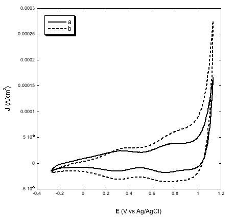
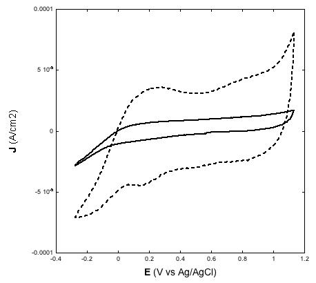
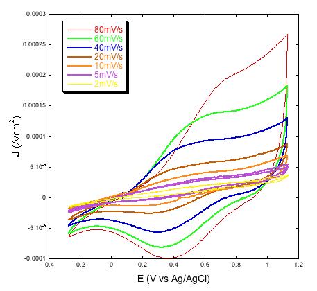
Another significant achievement of the deposition method here presented was the production of thin film electrodes of NiO displaying electroactivity throughout the whole film in both aqueous (Figure 2) [31,38,39] and non-aqueous (Figure 3) electrolytes [23,32,33], and creating an effective electrical contact at the NiO/FTO interface. This is proved by the direct proportionality between the extent of current density associated with the reversible oxidation of NiO [32,39] and NiO electrode thickness (Figures 2 and 3, left plots). Such a correlation indicates the occurrence of percolation between the nanoparticles sintered according to the scheme of Table 2, as well as a satisfactory mechanical adhesion of the NiO film at the FTO/glass substrate [24]. At the microscopic level interparticle percolation and interfacial adhesion would allow the transfer of the electronic charge carriers between adjacent nanoparticles and through the NiO/FTO interface, respectively.
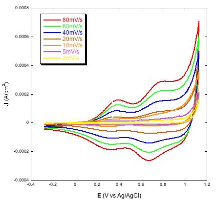
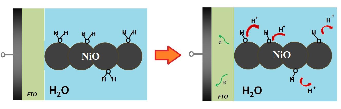
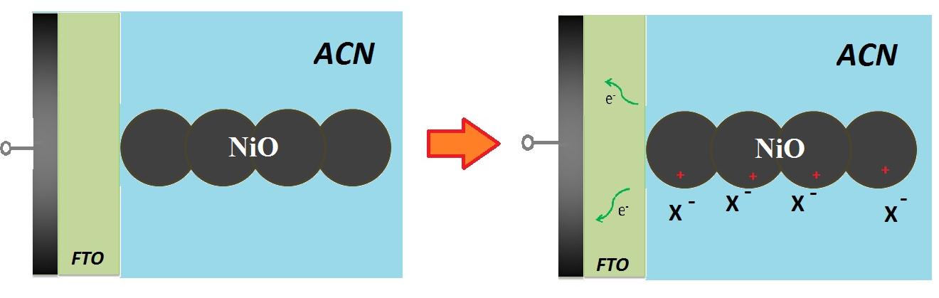
Similar to other types of NiO samples for p-DSCs [23,24,34,38] also the electrodes prepared via screen printing of the paste with the new composition here used show linearity between the height of the current peaks and scan rate (Figures 2 and 3, right plots) [29,31,32,39]. As previously outlined [38], such a finding is indicative of the occurrence of a surface confined event that controls the kinetics of the redox process based on the change of NiO oxidation state [22]. In aqueous electrolyte the electrochemical processes originating the voltammetric profiles of Figures 2 and 3 have been attributed to the redox reactions [22]:
NiO(OH)m→ NiOO(OH)m−1 + e− + H+ {1}
NiOO(OH)m−1→ NiOO2(OH)m−2 + e− + H+ {2}
as visualized in Figure 4, and, in organic electrolyte, to the redox reactions [22]:
NiO + m ClO4−→ Ni(II)1−mONi(III)m(ClO4)m + m e− {3}
Ni(II)1−mONi(III)m(ClO4)m + m ClO4− → Ni(II)1−mONi(IV)m(ClO4)2m + m e− {4}
as visualized in Figure 5.
Processes {2} and {4} occur at larger values of applied potential with respect to processes {1} and {3}. When the open circuit potential Voc of the three electrode cell having screen printed NiO film as working electrode is examined in the different experimental conditions (Table 3), a much stronger dependence of Voc with NiO film thickness (l) is observed in aqueous electrolyte with respect to the corresponding situation in anhydrous environment. Voc values were obtained prior to any polarization leaving the cell in a still position till the potential value became stable and the equilibrium condition was then reached. The increase of Voc with l in aqueous electrolyte is ascribed to the phenomenon of surface hydration and/or protonation as observed with surface spectroscopic techniques [39]. In contact with water the state of charge of the NiO surface is altered and, in absence of electrode polarization, hydration/protonation of NiO surface will occur at a much larger extent in the thicker film by virtue of its larger surface area with respect to the thinner film. This is a consequence of the mesoporous nature of this type of electrode (Figure 1). Apparently, the increase of NiO film thickness brings about the formation of an electrochemical double layer at the NiO/FTO interface which is enriched of positive charges on the electrode side with respect to the thinner NiO film having a smaller contact area. The increase of the oxidation potential Vox [corresponding to the realization of process {2} with current peak at the larger potential (Figure 2, left frame)] with film thickness in aqueous electrolyte is consistent with the increase of the degree of protonation in passing from thinner to thicker NiO electrode. In fact, a more positively charged surface will tend less to undergo a surface confined process of oxidation the charge compensation mechanism of which consists in the actual deprotonation of electrode surface (Eqs. 1 and 2). In anhydrous environment the open circuit potential is practically insensitive to the variation of NiO electrode thickness and then to the surface of the contact area itself. This implies the absence of a charge transfer process the extent of which is surface area dependent when the electrochemical double layer is formed in non-aqueous electrolyte.
Due to the existence of different interfacial processes in passing from aqueous to organic electrolyte in the condition of open circuit and during the process of NiO oxidation, we have considered the determination of electrochemical impedance spectra as most appropriate investigative tool for the analysis of the electrical parameter that characterize the NiO based electrochemical interfaces as well as the electron transport properties of screen printed NiO films under diverse conditions of polarization and different electrolytes. The electrochemical impedance spectra of NiO in the two different electrolytes at the potential of open circuit are presented in Figures 6 and 7 when NiO films differed for the value of thickness (l). The equivalent circuit that has been here proposed for the fit of the experimental impedance spectra at the potential of open circuit is schematically represented in Figure 8.
The proposed circuital model is characterized by the series connection of two interfacial elements constituted by the parallel connection of a resistance with a constant phase element. The latter represents a capacitance with non ideal geometrical features [41] like the present case of electrodes with highly open morphologies (Figure 1). In Figure 8 Rel, RFTO and Rtot are resistive terms which refer respectively to the ohmic resistance of the electrolyte, the sum of transport resistance (ohmic) through FTO layer and charge transfer resistance (non ohmic) at FTO/NiO interface, and the sum of transport resistance (ohmic) through NiO mesoporous layer and charge transfer resistance (non ohmic) at NiO/electrolyte interface. The capacitive terms CPEFTO and Cμ refer to the capacitances of the double layers created at the interfaces FTO/NiO and NiO/electrolyte, respectively, when the cell is in open circuit condition.
In both electrolytes the total resistance of screen printed NiO at Voc is quite high being in the order of 105 Ω. This stems from the poor conductivity of NiO in the pristine state [42] due to the low concentration of mobile charge carriers in the metal oxide when this is not polarized. As previously stated, the element Rtot is associated to the intrinsic transport properties of the oxide layer (it can be indicated with Rtrans) as well as the charge transfer resistance, Rct, through the metal oxide/electrolyte interface. In the fitting process the need of utilizing circuital elements with non ideal features does not render feasible the separated determination of Rtrans and Rct. Therefore, only their linear combination sum can be obtained for the mesoporous film of NiO. The other resistive term RFTO results always smaller than Rtot but it still presents a generally high value being in the order of few k Ω (Table 4). Similar to Rtot, the electrical resistance RFTO contains a linear combination of an ohmic term and an interfacial contribution that cannot be quantified separately. As a general consideration, the term Rtot which refers to NiO, includes two resistive contributions: (i) the resistance associated to the transport of charge through the NiO film (Rtrans, corresponding to the ohmic term contained in Rtot), and (ii) the resistance associated to the charge transfer through the interface NiO/electrolyte (Rct, corresponding to the non ohmic term in Rtot). The resistive ohmic term (i) increases with film thickness l and decreases upon augmentation of the concentration of charge carriers (the latter quantity increases upon NiO film oxidation since such an electrochemical process consists of the injection of holes in the metal oxide) [38], whereas the resistive non ohmic term (ii) diminishes with l for a mesoporous electroactive layer due to the fact that an increase in l brings about the increase of the surface area A for the NiO/electrolyte interface, i.e. the contact area between the metal oxide and electrolyte by virtue of the mesoporous nature of the electroactive NiO layer. In aqueous environment at Voc, the variation of Rtot with NiO film thickness is consistent with the fact that Rtot is now principally controlled by the omic term (i) associated to bulk charge transport within the NiO film, i.e. Rtot increases with l (Table 4). Under the same conditions of potential and electrolyte, the correspondingly increase of Cμ with the increase of l (Table 4) would indicate the direct dependence of Cμ on the surface area A of the NiO electrode/electrolyte interface being A α l for mesoporous electrodes as the ones here considered (Figure 1). Moreover, in the process of electrochemical double layer formation at the NiO/aqueous electrolyte interface, one has to consider the possible chemical reactions of oxide hydration and/or hydroxylation which necessarily lead to an alteration of the surface charge density on the metal oxide [39], as well as the change of crystalline phase following the occurrence of the electrochemical oxidation of NiO in water-based electrolytes as verified with XPS [39]. In organic electrolyte at open circuit potential, the observed decrease of Rtot with l (Table 4) forces us to suppose that Rtot is now dominated by the surface term (ii), i.e. the non ohmic resistive term (vide supra), which decreases with film thickness for the larger extension of the surface area of contact between electrode and electrolyte for the thicker film (l = 4 μm) with respect the thinner one with l = 2 μm. As previously outlined, the increase of A with l is consequence of the mesoporosity of this type of electrodes (Figure 1). The quasi constancy of the capacitive term Cμ with l at Voc in non-aqueous organic electrolyte (Table 4) is not of easy and straightforward interpretation. In fact, the lack of a clear dependence of Cμ on l at both Voc (Table 4) and Vox (Table 5) seems to be a consequence of the formation of an electrochemical double layer which involves the participation of the underlying FTO substrate together with NiO when the oxide gets thinner in non-aqueous electrolyte. This situation would be a consequence of the non-uniform coverage of the FTO substrate by the thinner film of nanoporous NiO (Figure 9). This supposition is partially supported by recognizing that also the capacitive term CPEFTO which refers to the FTO/NiO interface is more poorly dependent on l with respect to the same parameter evaluated in water-based electrolyte (Table 4).
From the comparative analysis of the data reported in Table 4 we conclude that contacting NiO with water electrolyte alters in a very significant way the state of superficial charge on the oxide with respect to an inert organic electrolyte and it is strongly dependent on NiO film thickness. In organic electrolyte the charge actually present on NiO surface is much smaller than that localized on the surface of NiO immersed in aqueous electrolyte at open circuit potential. This is evident from the data presented in Table 3: they reveal the lack of any dependence of Voc on l for the NiO/organic electrolyte interface due to the participation of underlying FTO, whereas Voc increases with l in aqueous environment for the specific charging of NiO interface by its interaction with water taking into account the increase of A with l [38]. This implies that the FTO surface directly exposed to organic electrolyte contributes quite considerably in the determination of the value of Voc as well as the interfacial capacitance at the electrode/organic electrolyte interface rendering the influence of NiO film thickness on Cμ very weak (Table 4). Additionally, it is expected that the interfacial term associated to the process of charge transfer through FTO/NiO interface will mostly contribute to the value of RFTO since the intrinsic resistance of FTO is in the order of few Ω when the layer is few μm thick as in this case [43]. As a consequence of surface protonation/hydration in aqueous environment (vide supra), the increase of NiO film capacitance in passing from the thinner to the thicker sample is coherent with the observed increase of open circuit potential (Table 3). In case of the thinner NiO film (l = 2 μm) in aqueous environment, it cannot be excluded the occurrence of NiO electrochemical erosion due to the metal oxide reaction of corrosion/dissolution with water [32,39], and the possible effect of shunting due to the direct exposability of FTO to the electrolyte. This is partly supported by the steady decrease of the electrical current exchanged by NiO upon continuous cycling in aqueous environment (Figure 10).
This unwanted effect could be at the basis of the anomalously low value of Cμ and the strikingly high values of RFTO and CPEFTO when compared to the corresponding values in organic electrolyte (Table 4). Alternative equivalent circuits that took explicitly into account the effects of NiO corrosion/dissolution in aqueous electrolyte were not further considered for the fitting of EIS data obtained with the thinner NiO electrode. Upon NiO the oxidation impedance spectra (Figures 11 and 12) show a clear improvement of the charge transport properties of NiO as evidenced by the diminished values of the resistive electrical elements (Table 4, vide infra) that are present in the equivalent circuit model of Figure 13. This is evidenced by the conspicuous decrease of the resistive term Rtot (Table 4), which is caused by the increase of the concentration of mobile charge carriers in oxidized NiO. This is a common behaviour for nanostructured NiO as observed also in other types of NiO samples [29,30]. The recording of the impedance spectrum of NiO in the oxidized state was done after a step of chronoamperometry at the value of NiO oxidation potential that was determined by the analysis of NiO voltammogram (Table 3). The impedance measurement was carried out immediately after the end of the potentiostatic polarization (duration 3600 s) in order to avoid uncontrollable changes of the state of oxidation of NiO electrode prior to the impedance analysis.
The equivalent circuit utilized for the fitting of the impedance spectra generated by oxidized screen printed NiO (Figures 11 and 12) is based on the model of Randles, which includes the Warburg term ZW (Figure 13) [44]. The most striking difference between the two equivalent circuits here proposed (Figures 8 and 13) is the presence of the electrical elements RFTO and CPEFTO that are associated to the FTO/NiO interface in the model relative to non polarized NiO. Such additional terms are related to the scarce conductivity of non-polarized NiO since in the pristine state such an oxide is a poor conductor (Figure 13 and Table 4) with semiconducting features [42]. Consequently, the FTO/NiO interface can be reasonably visualized as a barrier of the type metal/semiconductor with rectifying Schottky properties when NiO is in the unpolarized state. This is equivalent to say that pristine nonpolarized NiO is acting as an electron blocking layer [45]. The increase of NiO conductance following the electrochemical oxidation [this is evidenced by the drastic reduction of Rtot in passing from pristine to oxidized (105 Ω vs 102 Ω, Tables 4 and 5), vide infra] creates a sufficiently high number of charge carriers in NiO that do impart quasi metallic features in oxidized NiO. Because of this change of conductance, oxidized NiO ceases to act as an electron blocking layer in correspondence of the FTO/NiO interface and barrier effects are no longer generated at this surface of discontinuity. The introduction of the Warburg term ZW in the circuit of Figure 13 is representative of the mixed character of the charge carriers which are electronic holes and charge compensating anions "namely OH- in aqueous electrolyte (Eqs. 1 and 2), and ClO4- in the organic electrolyte (Eqs. 3 and 4) in oxidized NiO. This is somewhat similar to the situation of intercalation materials for charge storage which are based on transition metal compounds: the electronic charge localized within the electronic structure of the solid is accompanied by charge compensating ions located in interstitial sites or in between Van der Waals layers in order to preserve electroneutrality [40,46]. The two different types of carriers in oxidized NiO possess mobilities that are conditioned reciprocally and in the analysis of the charge transport properties of oxidized NiO the motion of ions has to be also taken into account through the Warburg term which is of diffusive nature [47]. The resistive (RZw) and capacitive (CZw) terms incorporated in the Warburg element (Table 5) are associated to the presence of the charge compensating ions that can be localized either on the electrode surface or within the structure of oxidized NiO [40]. The resistive term RZw is systematically 2-3 times higher than the electronic resistive term Rtot in both types of electrolytes (Table 5) for the involvement of the transport of larger mass charge carriers having ionic nature (see mechanisms of charge compensation in Eqs. 1-4).
At Vox the concentration of mobile charge carriers in NiO increases dramatically with respect to the oxide in the pristine, as deposited state at Voc as verified by the drastic diminution of Rtot in passing from Voc to Vox, independent of the nature of the electrolyte (Tables 4 and 5). The capacitance Cμ also decreases considerably upon shift of the applied potential from Voc to Vox when NiO is interfaced with both types of electrolytes. The occurrence of fast charge transfer processes through NiO/electrolyte interface and fast transport through oxidized NiO (Table 5) impede the accumulation of charge and then the building up of charged double layers at the oxidized electrode/electrolyte interface. Upon increase of film thickness l, the Rtot of oxidized NiO increases in organic electrolyte whereas the opposite trend is determined in aqueous electrolyte (Table 5). When the dual origin of the Rtot term is considered by taking into account the inclusion of the two terms Rtrans (i) and Rct (ii) (vide supra), we interpret the decrease of Rtot with l in water based electrolyte as a consequence of the stronger dependence of Rtot on the interfacial resistive term (ii) with respect to the bulk transport term (i), the nonlinear ohmic term Rct being inversely proportional to the extent of the area of oxidized NiO/electrolyte interface. In a regime of relatively high concentration of electrochemically injected charge carrier as verified at Vox, the total resistance of oxidized NiO is then controlled by the capability of the film to transfer charge through the interface with the electrolyte rather than to the capability of transporting charge through the oxide film. This consideration is consistent with the observation of a linear relationship between the amplitude of the oxidation peaks in the voltammograms of NiO and the applied scan rate (Figures 2 and 3). Such a trend is indicative of electrochemical processes the rate determining step of which is surface confined [48], and is commonly verified in the solid state electrochemistry of NiO [11,29,32,38,39]. Different to Rtot, the second resisitive term RZw which appears in the model of equivalent circuit (Figure 13) identified for the fitting of EIS data of oxidized NiO (Figures 11 and 12), is associated to the charge transport of ionic carriers through NiO film. To preserve electroneutrality the film of oxidized NiO requires the uptake of negatively charged compensating ions (Equations 3 and 4, Figure 5), or the release of positively charged species (Equations 1 and 2, Figure 4). Therefore, this resistive term characteristic of NiO in the sole oxidized version is influenced by the nature of the actual species compensating the charge of the electrochemically injected holes (Figures 2 and 3). Since charge transport in oxidized NiO involves ClO4- anions in organic environment (Figure 3), the ionic resistance associated to ClO4- motion within oxidized NiO will result generally higher that that originated by OH- ions in water electrolyte for the larger size of perchlorate with respect to the hydroxide anion. The variation of RZw with film thickness l in water based electrolyte has an opposite trend in comparison to the one observed for Rtot (Table 5). This stems from the fact that RZw is exclusively a through-bulk transport term which must increase in a directly proportional manner with l, i.e. is an extensive term which increases with the amount of oxidized NiO deposit. The increase of Cμ and CZw with l in aqueous electrolyte (Table 5) is due to the same reasons justifying the observed trend of Cμ with l in pristine NiO at Voc (Table 4, vide supra).
At Vox the behavior of Rtot with the variation of film thickness l in organic electrolyte is opposite to the trend determined in aqueous environment (Table 5). This would indicate the stronger influence of the bulk transport term (i) with respect to the interfacial contribution (ii) in presence of large concentration of electrochemically injected holes. The latter process is realized when NiO film is oxidized at applied potential larger than 0.1 V vs Ag/AgCl (Figure 3). When the dependence of the voltammogram shape on NiO electrode thickness in organic electrolyte is analyzed (Figure 3, left plot), the characteristic oxidation peaks of NiO are very ill-defined for the thinner NiO sample (l = 2 μm) with respect to the thicker one with l = 4 μm. Such a behavior in organic electrolyte, would indicate that the 2 μm thick film of oxidized NiO, i.e. the thinner sample, does not cover completely and in a uniform way the underlying FTO substrate leaving the latter in contact with the electrolyte (shunt effect) [RZw and references therein]. This was verified by mapping the atomic composition of the surface of 2 μm thick NiO sample (Figure 9). The surface elemental analysis conducted with SEM revealed parts of FTO exposed to the electrolyte through the visualization of the presence of Sn atoms on the external surface of the sample (Figure 9, bottom plot). We believe that the anomalously high values of Cμ, CZw and RZw for the 2 μm thick film of oxidized NiO in organic solvent derives from the observed lack of uniform coverage of the FTO substrate as well as from the relatively low amount of surface charge on exposed NiO in organic ambient with respect to the aqueous electrolyte. In fact, the effect of the lack of uniformity of FTO coverage by NiO in water based electrolyte on the electrical parameters Cμ, CZw and RZw would not be as evidenced as in organic electrolyte because of the involvement of a much larger quantity of surface charge in oxidized NiO interfaced to the aqueous electrolyte. The latter statement is supported by the observation of larger amounts of charge exchanged by NiO during its oxidation in aqueous with respect to non-aqueous environment (comparison of the areas comprised by the voltammograms in Figures 2 and 3, which have been determined in analogous conditions of scan rate and film thickness).
The working principle of a p-DSCs operating with I3-/I- redox mediator and mesoporous NiO as photoactive cathode sensitized by the generic sensitizer D is represented in Figure 14 [13].
The dye-sensitized solar cells based on screen printed NiO cathodes have shown photoelectrochemical activity with the redox couple I3-/I- when the cathode was either in the bare state or in the sensitized state with ERY colorant (Figure 15 and Table 6). In this respect the photoelectrochemical behavior of the screen printed NiO samples here presented does not show any anomaly or particularity with respect to the photoelectrochemical performance of other types of mesoporous NiO thin films fabricated for solar energy conversion scopes and sensitized with ERY [13,23,29,30].
From the plots of Figure 16 it is found that the maximum output intensity is supplied at about 60% and 54% of the maximum output voltage for bare NiO and ERY-NiO cells, respectively. For practical applications it is desirable that beside high conversion efficiencies the DSCs supply the maximum output of power/intensity at the maximum output potential achievable, i.e. Voc, provided that these photoelectrochemical devices possess diode-like features [49].
It is here demonstrated for the first time that unsensitized screen printed NiO displays photoelectroactivity similar to conventionally and plasma sintered NiO films [24,50], or sol-gel NiO samples [51,52]. Bare screen printed NiO photocathode produces a photocurrent with a maximum of external quantum efficiency (or IPCE) equal to 5.2% at a wavelength of ca. 370 nm in the corresponding p-DSC with the parameters of Table 6. Upon sensitization with ERY the IPCE maxima of the p-DSC with ERY-NiO photocathodes are located at ca. 370 nm (originated from NiO self-absorption), and ca. 540 nm (originated from the absorption of anchored ERY) with IPCE values of 5% and 2%, respectively. This finding would indicate that the photoelectrochemical action spectrum of ERY in NiO based p-DSCs practically sums up with that of bare NiO (no synergic effect between the processes of photoholes injection at the different wavelengths). The same sample of screen printed NiO has been employed as whole transporting material in a perovskite solar cell of p-type [53] when NiO film thickness was comprised in the range 200-300 nm and CH3NH3PbI3 was the photoactive material. These preliminary results indicated an overall efficiency of 0.022% with a non-optimized cell configuration. Research on these new types of solar conversion devices is still ongoing. The electrochemical impedance spectra of the p-DSCs having screened printed NiO are shown in Figure 17. Data of Figure 17 were recorded in dark conditions and under 1 sun of illumination.
The model of equivalent circuit utilized for fitting the impedance data of Figure 17 is presented in Figure 18 with reference to the sole experiment carried out under 1 sun of illumination.
The values of the best fitting parameters in the equivalent circuit of Figure 18 have been listed in Table 7.
In the process of data fitting we have utilized the model proposed by Natu et al. [54,55] who considered the series connection of two interfacial descriptors, i.e. a parallel combination of a constant phase element CPE with a charge transfer resistance for both working and counter electrodes when an atomically thick insulating layer of alumina was first deposited onto the transparent conductive coating of FTO. Such an analogy led us to depict our screen printed electrode as an inhomogeneous film formed by layers with different compactness which is covered by mesoporous surface. The corresponding hole lifetime τh in illuminated bare and ERY-sensitized NiO is straightforwardly given by the product RINTER*Cμ [56]. From the best fitting parameters it is found τh = 96.5 ms for bare NiO photocathode, and τh = 42.4 ms for ERY sensitized NiO photocathode when electrode thickness is 4 μm. These findings represent comparatively lower values with respect to the ones found by Natu et al. [54] when NiO was purposely covered by an auxiliary layer of insulating oxide to prevent interfacial recombination when P1 was the dye-sensitizer.
Screen printed NiO films from a newly formulated precursor have been used as photocathodes for p-DSCs when NiO thickness was less than 5 μm. The resulting overall efficiencies did not reach 0.05% with erythrosine b as colorant and I3-/I- as redox mediator. Photocells fill factors were comprised in the range 30-40% whereas the maximum attainable photovoltage was 130 mV when the conversion device had a photoactive area of 0.25 mm2. Photoelectrochemical impedance measurements gave charge recombination resistance (RINTER) of NiO in the order of 101-102 Ω the lowest values of RINTER being associated to the most efficient cells. The resulting lifetime of the photoinjected holes (τh) was in the range 40 - 100 ms with the largest values of τh determined with the less performing p-DSCs. For the first time it has been reported on the photoelectrochemical activity of a screen printed NiO in the bare state. In absence of a redox species in the electrolyte, pristine NiO underwent solid state oxidation processes in the range 0.1 - 1.0 V vs Ag/AgCl. Repetitive electrochemical cycling of NiO in aqueous electrolytes brought about the dissolution of the oxide film itself due to the spontaneous formation of surface nickel hydroxide and the high wettability consequential to NiO nanoporosity. Depending on the state of oxidation, as deposited NiO behaved as insulator (total electrical resistance range: 1*105 < Rtot < 6*105 Ω) and hole conductor (20 < Rtot < 150 Ω) in the pristine and oxidized states, respectively. This led to the definition of different equivalent circuits to interpret the electrochemical impedance data. In the insulating state NiO apparently creates a barrier at the FTO/NiO interface which impedes further charges transfer. Rtot of NiO was defined as a resultant combination of two non-separable and independent terms referring to bulk transport and interfacial charge transfer. Rtot depended on the nature of the electrolyte and on NiO film thickness in a non-straightforward way due to the occurrence of NiO film detachment from FTO substrate in aqueous electrolyte upon continuous electrochemical cycling and the non-uniform coverage of FTO by the NiO sample with the lower thickness (2 μm).
The results presented in this work have been obtained within the framework of a research project supported by Regione Lazio and CHOSE. The authors acknowledge the financial support of Ateneo Sapienza (protocol no: 2011/VG1-C26A11PKS2). Moreover, D.D. gratefully acknowledges the financial support from Ministero dell’Istruzione dell’Università e della Ricerca-MIUR (project title: DSSCX; protocol no.: PRIN 2010–2011, 20104XET32). Authors thank Prof. Elizabeth Gibson and her team (School of Chemistry at the University of Nottingham, UK) for the realization of HR-TEM pictures and BET adsorption experiments. Authors are also indebted to Prof. Denis P. Dowling and his research group (School of Chemical and Bioprocess Engineering, Engineering and Materials Science Center, University College Dublin-UCD, Dublin, Ireland) for the realization of X-rays diffraction experiments. Dr. Francesco Mura at CNIS (Centro Di Ricerca per le Nanotecnologie Applicate All'Ingegneria, University of Rome La Sapienza), is gratefully acknowledged for the realization of surface elemental analysis with SEM facility.

![]()

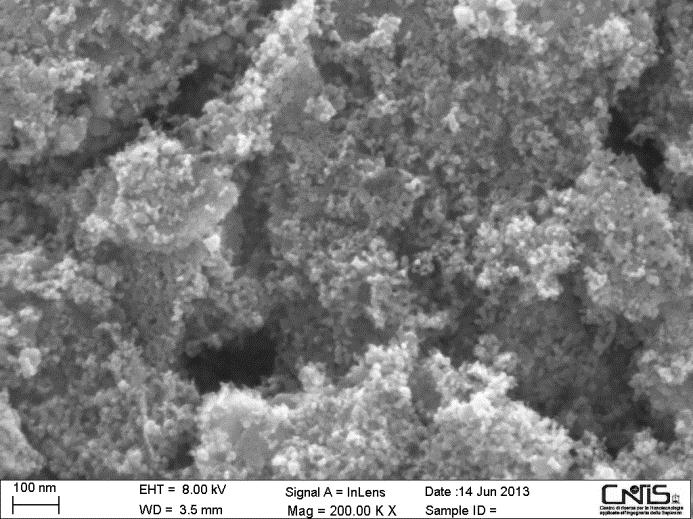 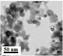 |
| Figure 1: Left: FE-SEM surface images of the screen printed NiO sample obtained from the paste with the chemical composition specified in Table 1 and utilizing the sintering procedure reported in Table 2. NiO film thickness was 4 µm; Right: high resolution TEM image of screen printed NiO sample |
  |
| Figure 2: Left: voltammograms of screen printed NiO electrodes with two different thickness values (a, full line: 2 µm; b, dotted line: 4 µm) at the scan rate of 10 mV s-1; Right: voltammograms of 4 µm thick NiO at various scan rates; Electrolyte is the same for both plots and consists of the water solution of 0.2 M KCl containing the phosphate buffer. Electrolyte composition: 0.2 M KCl, 0.01 M KH2PO4, 0.01 M Na2HPO4 in H2O |
  |
| Figure 3: Left: voltammograms of screen printed NiO electrodes with two different thickness values (full line: 2 µm; dotted line: 4 µm) at the scan rate of 10 mV s-1; Right: voltammograms of 4 µm thick screen printed NiO at various scan rates; Electrolyte is the same for both plots and consists of 0.2 M LiClO4 in 3-methoxy-propionitrile. |
 |
| Figure 4: Depiction of the mechanism of charge compensation during the electrochemical oxidation of screen printed NiO in aqueous electrolyte (Eqs. 1 and 2). Electrons flow from NiO to the charge collector through the FTO conductive substrate. Charge compensation consists in the loss of protons from oxide surface which is imaged as hydrated by the direct contact with water solvent [39] |
 |
| Figure 5: Depiction of the mechanism of charge compensation during the electrochemical oxidation of screen printed NiO in organic electrolyte (Eqs. 3 and 4). Electrons flow from NiO to the charge collector through the FTO conductive substrate. ACN refers to the electrolytic solvent (usually acetonitrile or 3-methoxy-propionitrile). The symbol X- indicates the anion of the supporting electrolyte (in the case here considered it represents ClO4-). Charge compensation could be localized either on the surface as indicated in the right picture (most common case for the oxidative electrochemistry of NiO) [29,30,30], or could consists of charge intercalation if the host oxide possesses a layered structure made of Van der Waals planes [40]. |
 |
| Figure 6: Impedance spectra of the three electrode cells having screen printed NiO as working electrode [red profile: l = 2 µm; blue profile: l = 4 µm]. Spectra were recorded at the potential VOC when the electrolyte was aqueous. The lines represent the corresponding interpolation curves determined with the equivalent circuit of Figure 8 (vide infra) |
 |
| Figure 7: Impedance spectra (red empty circles) of the three electrode cells having screen printed NiO as working electrode [l = (red profile) 2 µm, (blue profile) 4 µm]. Spectra were recorded at the potential VOC when the electrolyte was organic. The solid lines represent the corresponding interpolation curves determined with the equivalent circuit reported in Figure 8 (vide infra) |
 |
| Figure 8: Electrical equivalent circuit utilized to model the impedance spectra of screen printed NiO polarized at open circuit potential Voc when the metal oxide constitutes the working electrode of a three-electrode cell. The model refers to the cell utilizing either aqueous (Figure 6) or organic (Figure 6) electrolyte. The meaning of the symbols is reported in the text |
   |
| Figure 9: Top: surface morphology of a 2 µm thick NiO film deposited onto FTO as determined with SEM; Center: green visualization of Ni atoms on the same surface portion of the SEM picture at the top; Bottom: blue visualization of Sn atoms on the same surface portion of the SEM picture at the top. Scale is the same in all three pictures |
 |
| Figure 10: Effect of continuous cycling on the voltammogram of screen printed NiO. NiO thickness: 2 µm; scan rate: 10 mV s-1. Same electrolyte as in the experiments of Figures 2 and 6 |
 |
| Figure 11: Impedance spectra of the three electrode cell having screen printed NiO as working electrode [l = (red profile) 2 µm, (blue profile) 4 µm]. Spectra were recorded at the potential Vox (see Table 3) when the electrolyte was aqueous. The lines represent the corresponding interpolation curves determined with the equivalent circuit of Figure 13 (vide infra) |
 |
| Figure 12: Impedance spectra of the three electrode cell having screen printed NiO as working electrode [l = (red profiles) 2 µm, (blue profiles) 4 µm]. Spectra were recorded at the potential of oxidation Vox (see Table 3) when the electrolyte was organic. Lines represent the corresponding interpolation curves determined with the equivalent circuit of Figure 13 (vide infra) |
 |
| Figure 13: Electrical equivalent circuit utilized to model the impedance spectra of screen printed NiO polarized at Vox (for the values see Table 3) when the metal oxide constitutes the working electrode of a three-electrode cell. The model refers to the cell utilizing either aqueous (Figure 11) or organic (Figure 12) electrolyte. The meaning of the symbols is reported in the text |
 |
| Figure 14: Graphical representation of the energy levels and the mechanisms at the basis of the operation of a NiO based p-DSC. Bent arrows represent the movements of the electrons following the absorption of light by the anchored dye. Double arrow (1) shows the amplitude of VOC. Dotted arrow (2) indicates the electron transfer that occurs for the recombination between the reduced form of the redox mediator (the photoproduct) and the NiO hole in VB. Dotted arrow (3) indicates the electron transfer that leads to the recombination between the photogenerated reduced dye (D-, a species with transient character) and a NiO hole in VB |
 |
| Figure 15: Characteristic JV curves of the p-DSCs employing (black profile) bare NiO, and (orange profile) ERY-sensitized NiO as photocathodes; Geometry irradiation and incident intensity were the same for the two cells |
 |
| Figure 16: Profiles of output intensity Iout vs output voltage Eout for the two p-DSCs with the characteristic JV curves of Figure 15; Black and red profiles refer to the photocells with bare and ERY-sensitized NiO photocathodes, respectively |
  |
| Figure 17: EI spectra recorded at Voc for the p-DSCs with screen printed NiO photocatode (l = 4 µm). The latter was either bare NiO (full circles) or ERY-sensitized NiO (empty circles). Spectra were recorded under 1 sun of illumination (left plot), and in dark conditions (right plot) |
 |
| Figure 18: Electrical equivalent circuit utilized to model the impedance spectra of the p-DSCs with screen printed NiO at Voc in both bare and ERY sensitized states (for the respective values of Voc see Table 6). Symbols RS, RCE, CPE CE and RINTER refer to the series resistance of the cell, the charge transfer resistance at the counter electrode/electrolyte interface, the constant phase element of capacitive nature related to the electrochemical double layer at the counter electrode/electrolyte interface, and the interfacial resistance (recombination resistance) at the NiO electrode/electrolyte interface, respectively. |
Step 1 |
6g of NiO nanopowder are grinded with 2mL of glacial acetic acid for 5 min (final volume of mixture: 2 mL) |
Step 2 |
Addition of 1mL of H2O to the mixture obtained after Step 1 and grinding for 1 min. This succession is repeated 5 times (final volume of mixture: 7 mL) |
Step 3 |
Addition of 1mL of ethanol to the mixture of Step 2 and grinding for 1 min. This succession is repeated 15 times (final volume of the mixture: 22 mL) |
Step 4 |
Addition of 2.5mL of ethanol to the mixture of Step 3. This succession is repeated 6 times (final volume of the mixture: 37 mL) |
Step 5 |
Transfer of the paste of Step 4 to a beaker using 100 mL of ethanol (final volume of the mixture: 137 mL) |
Step 6 |
The mixture of Step 5 is stirred 1 min, successively sonicated for 2 min and finally stirred again for 1 min |
Step 7 |
Addition of terpineol (20 g) |
Step 8 |
The mixture of Step 7 is stirred 1 min, successively sonicated for 2 min and finally stirred again for 1 min |
Step 9 |
Addition of a solution of ethyl cellulose to the mixture of Step 8. The added solution is formed by adding 3 g of ethyl cellulose in 30g of a 10% v/v solution of ethanol in aqueous solvent |
Step 10 |
The mixture of Step 9 is stirred 1 min, successively sonicated for 2 min and finally stirred again for 1 min. This succession of 4 min is repeated 3 times |
Step 11 |
Slow evaporation of the volatile components of the resulting mixture: The mixture of Step 10 is placed on hot plate at 50 oC for 9 hours. After then the NiO nanoparticles paste is cooled down to ambient temperature and ready for being utilized in the screen-printing mode of deposition |
| Table 1: Procedure of the preparation of the paste for the screen-printing deposition of NiO | |
Step 1 |
Pre-heating of the NiO deposits in oven at 100 oC (duration: 15 mins) |
Step 2 |
Gradual heating of the deposits up to 450 oC utilizing a thermal ramp (heating rate: 15 oC min-1) |
Step 3 |
Sintering at 450 oC (duration: 30 mins) |
Step 4 |
Cooling down of the sintered deposits to room temperature in closed oven utilizing the system of internal ventilation of the oven |
Step 5 |
Storage in dark conditions under controlled atmosphere |
| Table 2: General procedure of sintering for the three different NiO deposits after screen-printing deposition | |
Thickness / µm |
Aqueous electrolyte |
Organic electrolyte |
||
Voc / V |
Vox/ V |
Voc/ V |
Vox/ V |
|
2 |
-0.05 |
0.90 |
0.10 |
0.80 |
4 |
0.20 |
0.80 |
0.10 |
0.85 |
| Table 3: Open circuit potential values (Voc) and potential of maximum current of oxidation (Vox) for screen-printed NiO electrodes in aqueous and non-aqueous electrolytes. Potential values are referred to the standard potential of the redox couple Ag/AgCl | ||||
NiO film thickness / µm |
aqueous electrolyte |
organic electrolyte |
||
2 |
4 |
2 |
4 |
|
Equivalent circuit element |
||||
Rtot / kΩ |
269.2 ± 54.4 |
607.1 ± 11.8 |
297.9 ± 45.6 |
123.8 ± 25.8 |
Cµ / µF |
74 ± 11 |
488 ± 59 |
208 ± 19 |
195 ± 29 |
RFTO / Ω |
10061 ± 3875 |
3966 ± 260 |
3351 ± 302 |
4175 ± 603 |
CPEFTO / µF |
78.16 ± 5.00 |
16.65 ± 3.13 |
20.29 ± 1.02 |
15.76 ± 2.83 |
| Table 4: Values of the electrical elements constituting the equivalent circuit that fits the EIS response of NiO thin film electrodes at Voc (Figures 6 and 7). The equivalent circuit fitting the experimental data in both types of electrolytes has been schematically represented in Figure 8 | ||||
NiO film thickness / µm |
aqueous electrolyte |
organic electrolyte |
||
2 |
4 |
2 |
4 |
|
Equivalent circuit element |
||||
Rtot / kΩ |
42.91 ± 2.45 |
27.19 ± 2.15 |
82.95 ± 13.05 |
131.6 ± 4.7 |
Cµ / µF |
0.096 ± 0.028 |
5.40 ± 1.62 |
0.338 ± 0.176 |
0.200 ± 0.030 |
RFTO / Ω |
73.12 ± 3.40 |
97.61 ± 2.35 |
439.7 ± 14.7 |
268.4 ± 5.6 |
CPEFTO / µF |
28.8 ± 1.4 |
77.1 ± 2.3 |
2040 ± 110 |
1160 ± 20 |
| Table 5: Values of the electrical elements constituting the equivalent circuit that fits the EIS response of NiO thin film electrodes at Voc(Figures 11 and 12). The equivalent circuit fitting the experimental data in both types of electrolytes has been schematically represented in Figure 9 | ||||
Sensitizer |
Voc / mV |
Isc / mA |
Jsc / mA cm-2 |
FF / % |
h / % |
- |
90 |
0.008 |
0.033 |
39.0 |
0.001 |
ERY |
127 |
0.026 |
0.103 |
33.4 |
0.004 |
| Table 6: Values of the photoelectrochemical parameters of interest for the p-DSCs based on screen printed NiO films (l = 4 µm) that have been deposited from a paste with the formulation here reported. The symbols Voc , Isc , Jsc , FF and h stand for open circuit potential, short circuit current, short circuit current density, fill factor and overall conversion efficiency. Data have been extracted from the JV curves in Figure 15 | |||||
ERY-sensitized NiO |
Bare NiO |
|
Equivalent circuit element |
||
Rs / Ω |
33.86 ± 0.13 |
19.84 ± 0.05 |
RCE / Ω |
92.95 ± 7.55 |
229.7 ± 16.4 |
CCE / µF |
103 ± 7 |
61 ± 2 |
RINTER / Ω |
614.1 ± 8.7 |
2098 ± 21 |
Cµ / µF |
69 ± 1 |
46 ± 1 |
| Table 7: Values of the parameters fitting the EIS spectra determined in the experimental conditions of Figure 17 at open circuit potential under 1 sun of illumination. The meaning of the symbols is given in the text with reference to the equivalent circuit of Figure 18 | ||